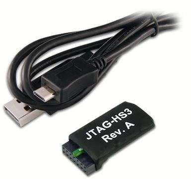
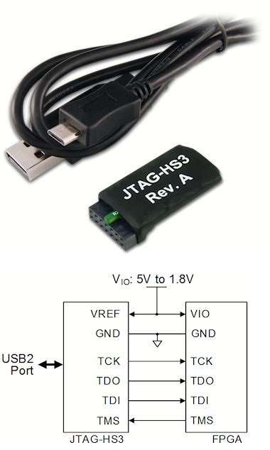
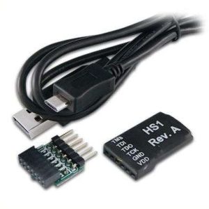
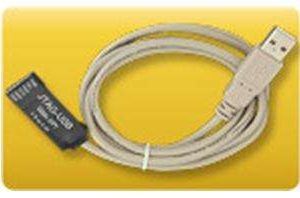
The JTAG HS3 is the newest member of our family of affordable high-speed Xilinx FPGA programming solutions. The HS3 builds on the successful JTAG HS1 by adding an open drain buffer to pin 14 allowing for the debugging of Xilinx Zync-SOC processors. It can be attached to target boards using Xilinx’s 2×7 connector*, and is compatible with all Xilinx tools, including iMPACT, Chipscope, and EDK.
When connected to a PC via a standard A to micro-USB cable, the JTAG HS3 receives its power from USB and can be recognized as a Digilent programming cable, even if the HS3 is not attached to the target board. The JTAG bus can be shared with other devices as the HS3’s signals are held in high-impedance, except when actively driven during programming. The HS3 is small and light, allowing it to be held firmly in place by the system board connector.
NOTE: This cable is not needed for Digilent FPGA boards as our boards are designed with this functionality natively.
* This is a unique programming header and is not compatible with the 1×6 MTE Digilent JTAG connector
- Small, complete, all-in-one JTAG programming/debugging solution for Xilinx FPGAs and SoCs
- Plugs directly into standard Xilinx JTAG header
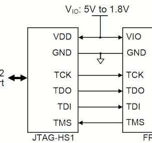
- Separate Vref drives JTAG signal voltages; Vref can be any voltage between 1.8V and 5V
- High-Speed USB2 port that can drive JTAG bus up to 30Mbit/sec (frequency adjustable by user)
- Compatible with Xilinx ISE® 14.1 and newer, Xilinx Vivado 2013.3 and newer
- Uses USB Micro-B connector
- Open drain buffer on pin 14 allows debugging software to reset the processor core of Xilinx’s Zynq® platform
User Manual HERE

